At AboutMechanics, we're committed to delivering accurate, trustworthy information. Our expert-authored content is rigorously fact-checked and sourced from credible authorities. Discover how we uphold the highest standards in providing you with reliable knowledge.
What Is Wafer-Level Packaging?
Wafer-level packaging refers to fabrication of integrated circuits by applying packaging around each circuit before the wafer on which they are fabricated is separated into individual circuits. This technique has grown rapidly in popularity in the integrated circuit industry due to advantages in terms of component size as well as production time and cost. A component fabricated this way is considered a type of chip scale package. This means that its size is nearly the same as that of the die inside it, on which the electronic circuitry is located.
Conventional manufacture of integrated circuits generally begins with production of silicon wafers upon which circuits will be fabricated. A pure silicon ingot is typically cut into thin slices, called wafers, which serve as the foundation upon which microelectronic circuits are built. These circuits are separated with a process known as wafer dicing. Once separated, they are packaged into individual components, and solder leads are applied to the package.
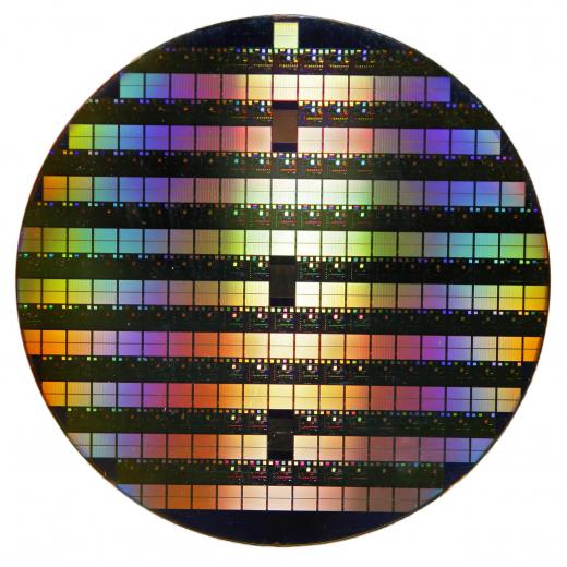
Wafer-level packaging differs from conventional fabrication in how the package is applied. Rather than splitting the circuits apart and then applying the packaging and leads before continuing on to testing, this technique is used to integrate multiple steps. The top and bottom of the package and the solder leads are applied to each integrated circuit before wafer dicing. Testing also typically takes place before wafer dicing.

Like many other common component package types, integrated circuits manufactured with wafer-level packaging are a type of surface-mount technology. Surface-mount devices are applied directly to the surface of a circuit board by melting solder balls attached to the component. Wafer level components can typically be used similarly to other surface mount devices. For example, they may often be purchased on tape reels for use in automated component placement systems known as pick and place machines.
A number of economic benefits can be achieved with the implementation of wafer-level packaging. It allows integration of wafer fabrication, packaging, and testing, thereby streamlining the manufacturing process. Reduced manufacturing cycle time increases production throughput and reduces cost per unit manufactured.
Wafer-level packaging also allows for reduced package size, which saves material and further reduces production cost. More importantly, however, reduced package size allows components to be used in a wider variety of advanced products. Need for smaller component size, especially reduced package height, is one of the main market drivers for wafer-level packaging.
Components fabricated with wafer-level packaging are used extensively in consumer electronics such as cell phones. This is largely due to market demand for smaller, lighter electronics that can be used in ways that are ever more complex. For example, many cell phones are used for a variety of functions beyond simple calling, such as taking photos or recording video. Wafer-level packaging has also been used in a variety of other applications. For example, they are used in automotive tire pressure monitoring systems, implantable medical devices, military data transmission systems, and more.
AS FEATURED ON:
AS FEATURED ON:

-
![Wafer-level packaging differs from conventional fabrication in how the package is applied.]() By: Vasily SmirnovWafer-level packaging differs from conventional fabrication in how the package is applied.
By: Vasily SmirnovWafer-level packaging differs from conventional fabrication in how the package is applied. -
![Wafer-level packaging has allowed cell phones, tablets and computers to shrink in size while adding capabilities.]() By: sepyWafer-level packaging has allowed cell phones, tablets and computers to shrink in size while adding capabilities.
By: sepyWafer-level packaging has allowed cell phones, tablets and computers to shrink in size while adding capabilities.


Discuss this Article
Post your comments